Draw the current-voltage characteristics for the device shown in figure between the terminal A and B.
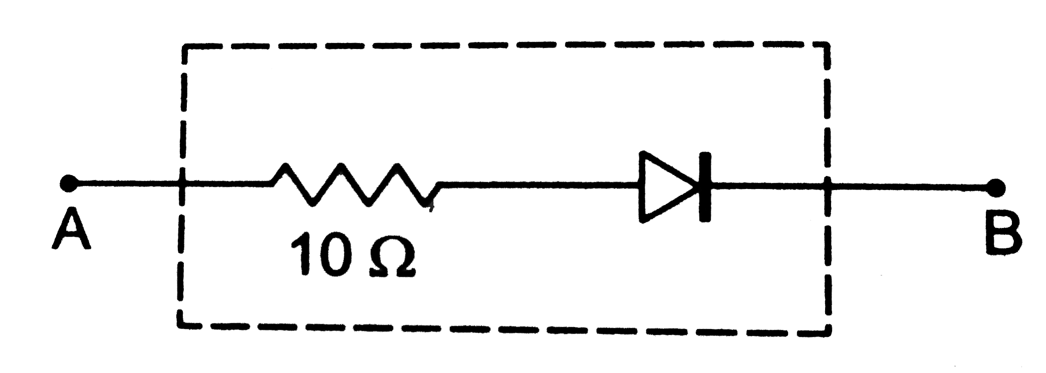

Drow yourself.
Topper's Solved these Questions
- SEMICONDUCTOR AND SEMICONDUCTOR DEVICESBook:HC VERMA ENGLISHChapter:SEMICONDUCTOR AND SEMICONDUCTOR DEVICESExercise:Question for short answer
Explore 11 Videos
- SEMICONDUCTOR AND SEMICONDUCTOR DEVICESBook:HC VERMA ENGLISHChapter:SEMICONDUCTOR AND SEMICONDUCTOR DEVICESExercise:objective II
Explore 8 Videos
- PHOTOMETRYBook:HC VERMA ENGLISHChapter:PHOTOMETRYExercise:All Questions
Explore 38 Videos
- SPEED OF LIGHTBook:HC VERMA ENGLISHChapter:SPEED OF LIGHTExercise:Question for short Answer
Explore 5 Videos
Similar Questions
Consider a box with three terminals on top of it as shown in figure.
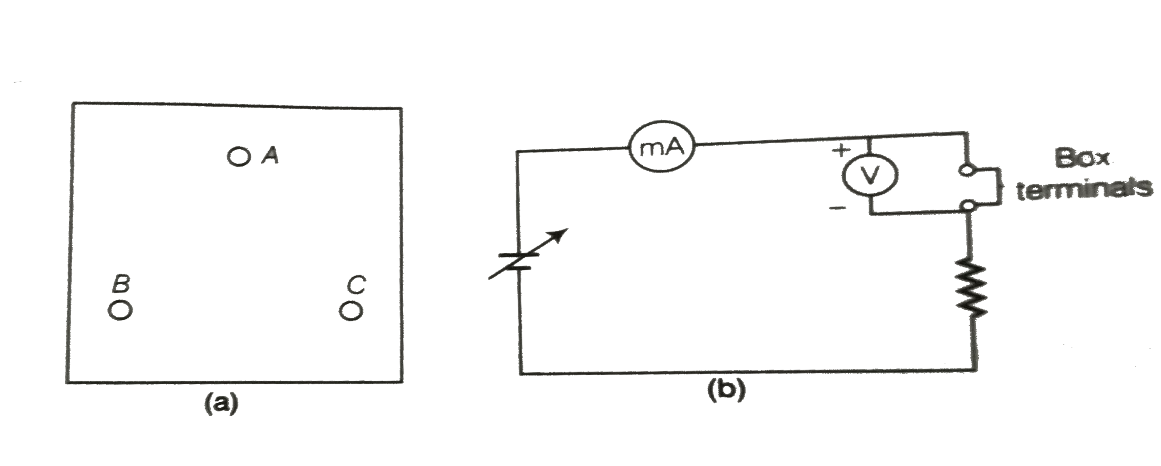
Three components namely, two germanium diodes and one resistor are connected across these three terminals in some arrangement
A student performs an experiment in which any two of these three terminals are connected in the circuit shown in figure.
The student obtains graphs of current-voltage characteristics for unknown combination of components between the two terminals connected in the circuit. The graphs are
(i) When A is positive and B is negative
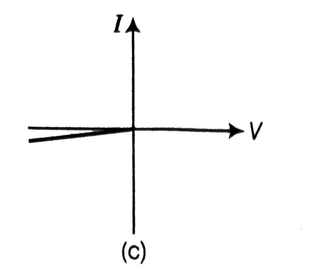
(ii) When A is negative and B is positive
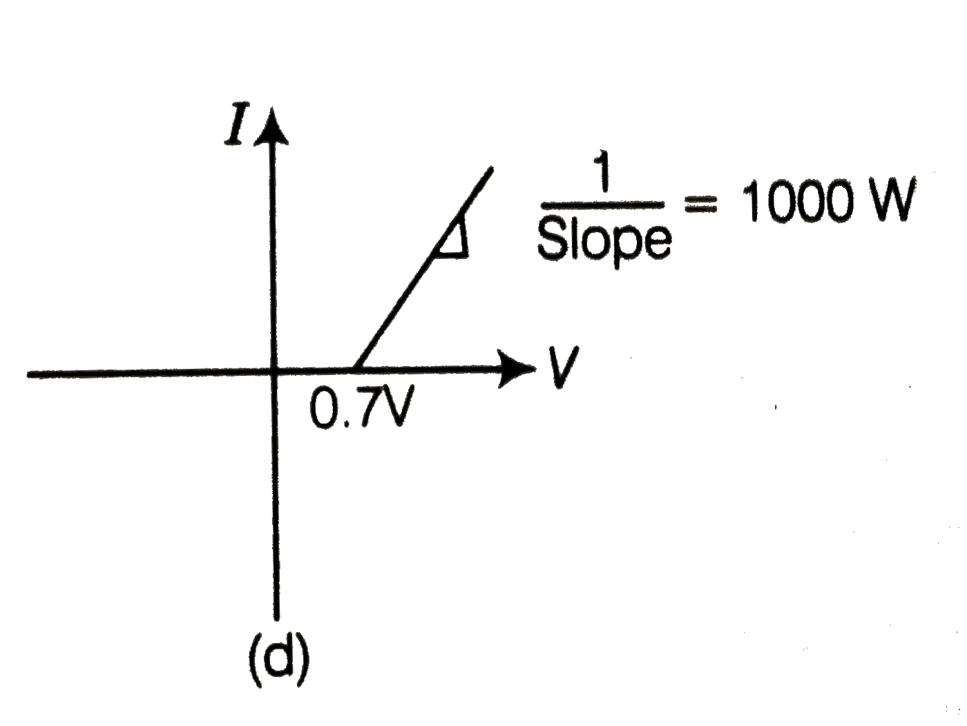
(iii) When B is negative and C is positve
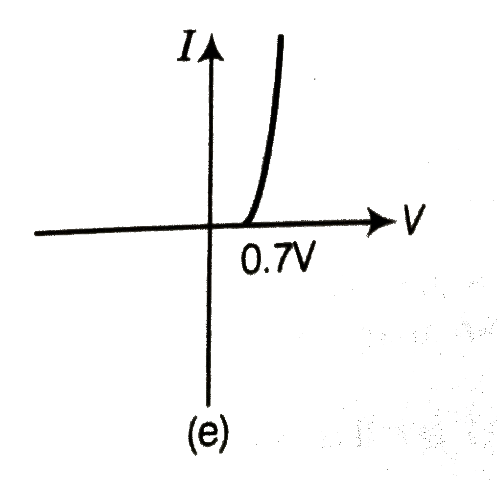
(iv) When B is positive and C is neagtive
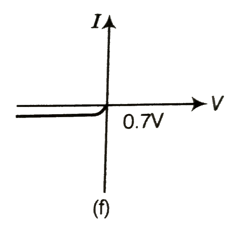
(v) When A is positive and C is negative
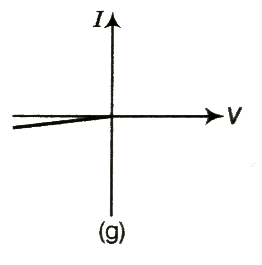
(vi) When A is negative and C is positive
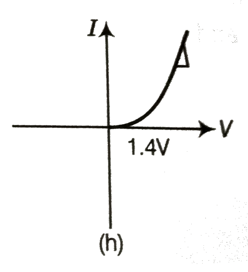
From these graphs of current − voltage characteristic shown in fig. (c) to (h) determine the arrangement of components between A, B and C.
View SolutionIdentify the correct characteristic feature shown by the given figures ?
View Solution
Knowledge Check
1-V characteristics of four devices are shown in figure.
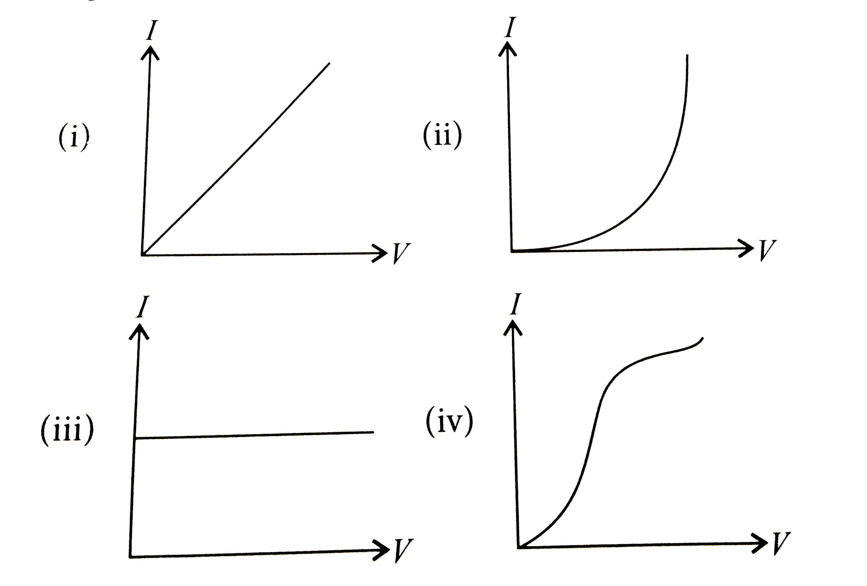
Identify devices that can be used for modulationA(i) and (iii)BOnly (iii)C(ii) and some regions of (iv)DAll the devices can be usedThe I-V characteristics shown in the figure represents
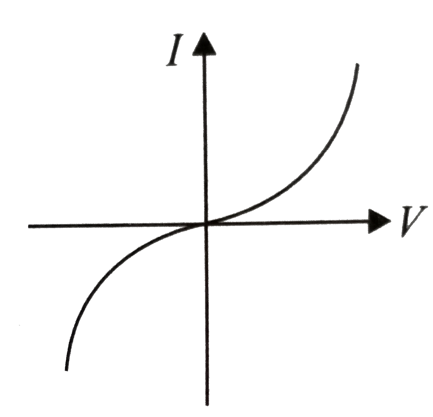 Aohmic conductorsBnon-ohmic conductorsCinsulatorsDsuperconductors
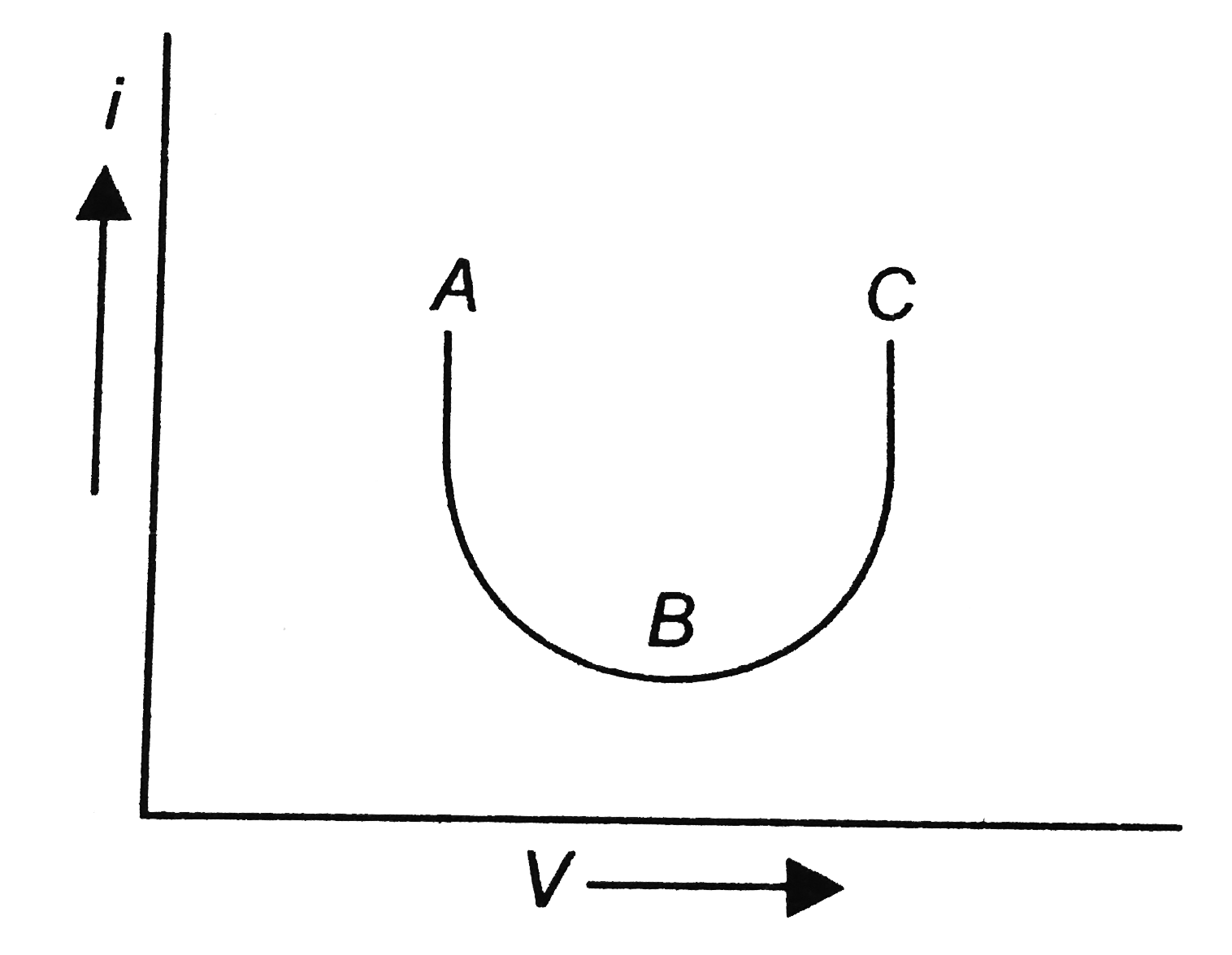
The current-voltage graph of a device is shown in figure. The resistance is negative in region.
View SolutionI-V characteristics of four devices are shown in figure.

Identify devices that can be used for modulation
View SolutionCalculate the resistance between the terminals A and B of the network shown in fig

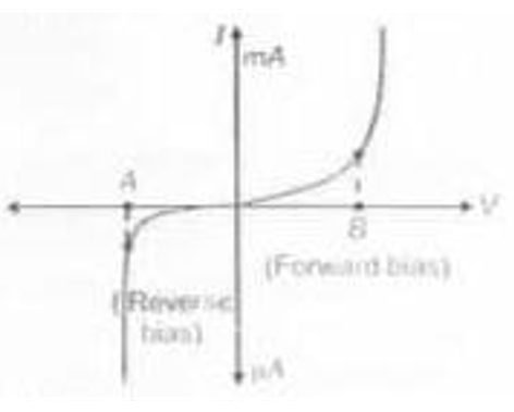
View SolutionIn the voltage current (V-l) characteristics of junction diode (figure) the point A and B corresponds to
View Solution1-V characteristics of four devices are shown in figure.

Identify devices that can be used for modulation
View SolutionThe time constant for LR circuit between the terminals a and b as shown in diagram is
View Solution
