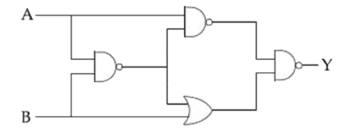
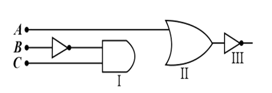
The output (X) of the logic circuit shown in figure will be

A
X=¯¯¯¯¯¯¯A⋅¯¯¯¯¯¯B
B
X=¯¯¯¯¯¯¯¯¯A⋅B
C
X=A⋅B
D
X=¯¯¯¯¯¯¯¯¯¯¯A+B
Video Solution
Text Solution
The correct Answer is:C
X=¯¯¯¯¯¯¯¯¯¯¯¯AB=A⋅B(i.e. AND gat)
If the output X of NAND gate is connected to the input of NOT gate (made from NAND gate by joining two inputs) from the given figure then we get back an AND gate.
|
Similar Questions
Knowledge Check
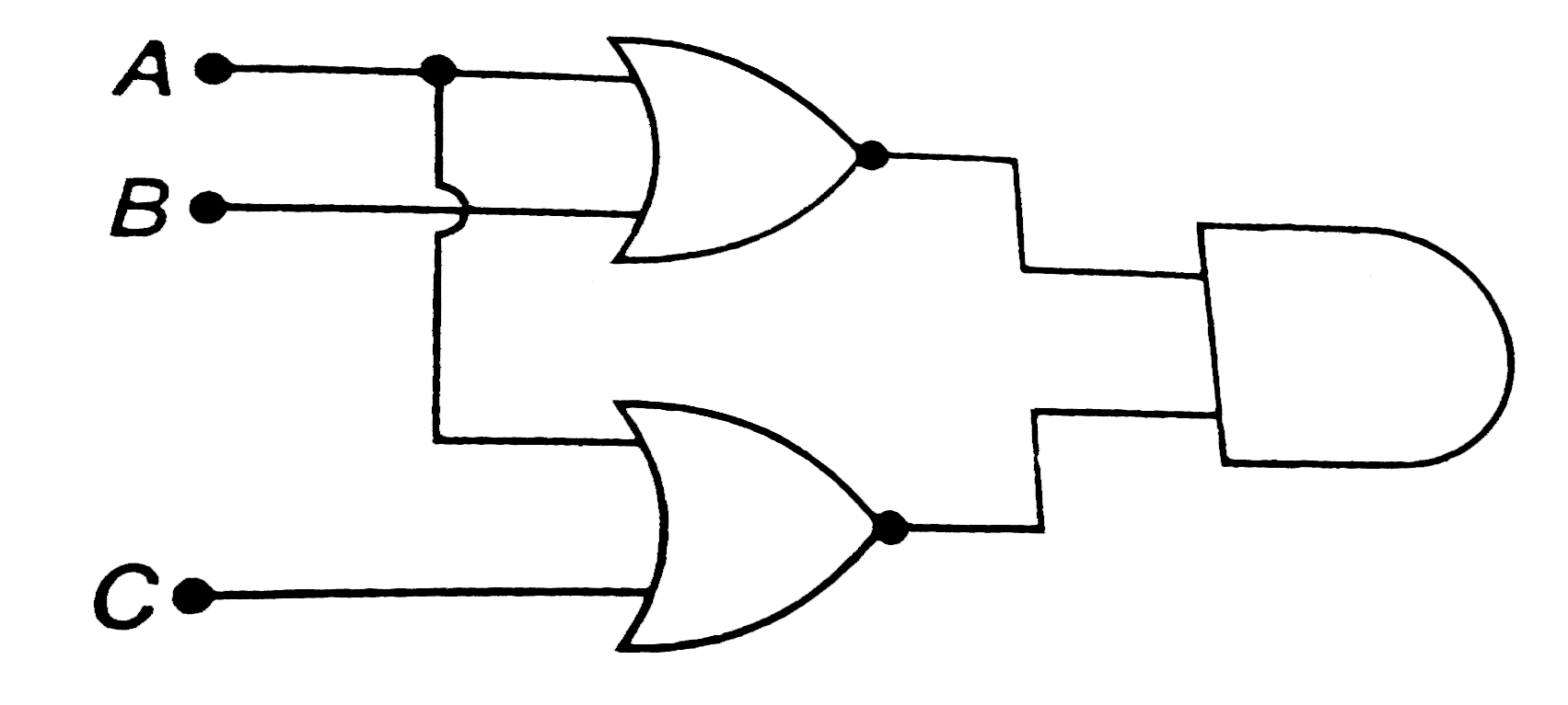
The output Y of the logic circuit as shown in figure is
 A(A+B)⋅¯¯¯CB(A+C)⋅¯¯¯CC(B+C)⋅¯¯¯ADA+B+C
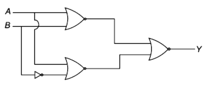
The output Y of the logic circuit as shown in figure is best represents as
 A¯¯¯A+¯¯¯¯¯¯¯¯¯B⋅CBA+¯¯¯B⋅CC¯¯¯¯¯¯¯¯¯¯¯¯¯¯¯¯¯A+B⋅CD¯¯¯¯¯¯¯¯¯¯¯¯¯¯¯¯¯A+¯¯¯B⋅C
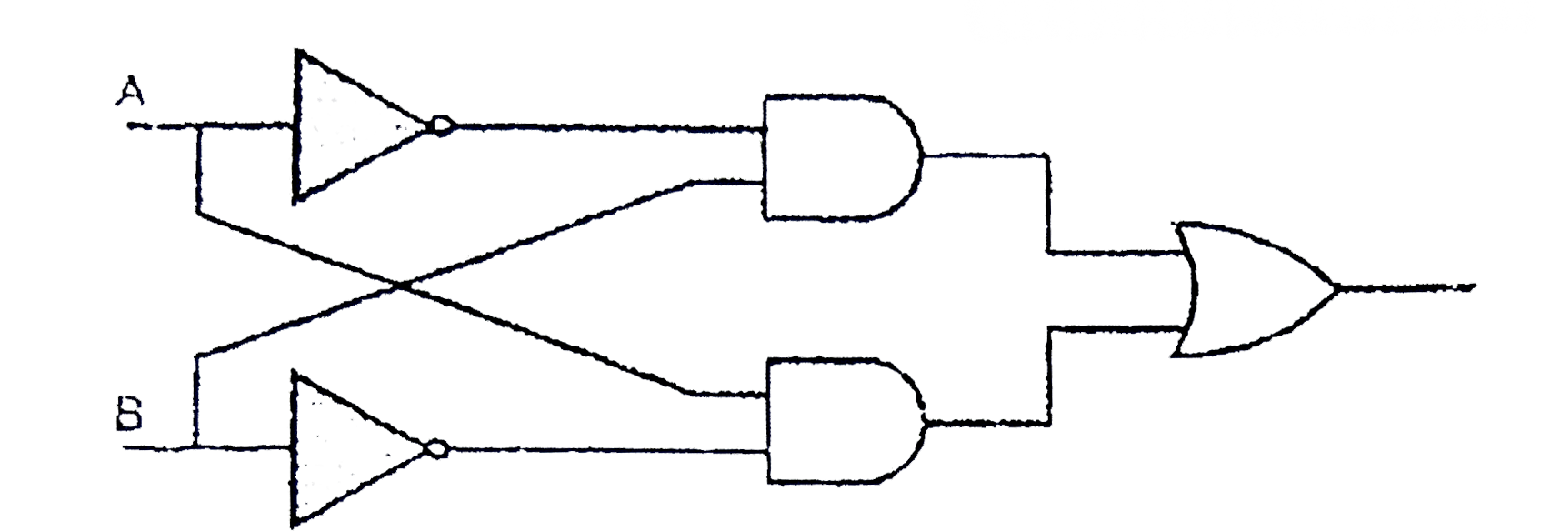
The outpout Y of the logic circuit shown in figure is best represented as
 A¯¯¯A+¯¯¯B.¯¯¯CB¯¯¯A+¯¯¯B.CC¯¯¯A+B.¯¯¯CD(¯¯¯A+¯¯¯B)C

