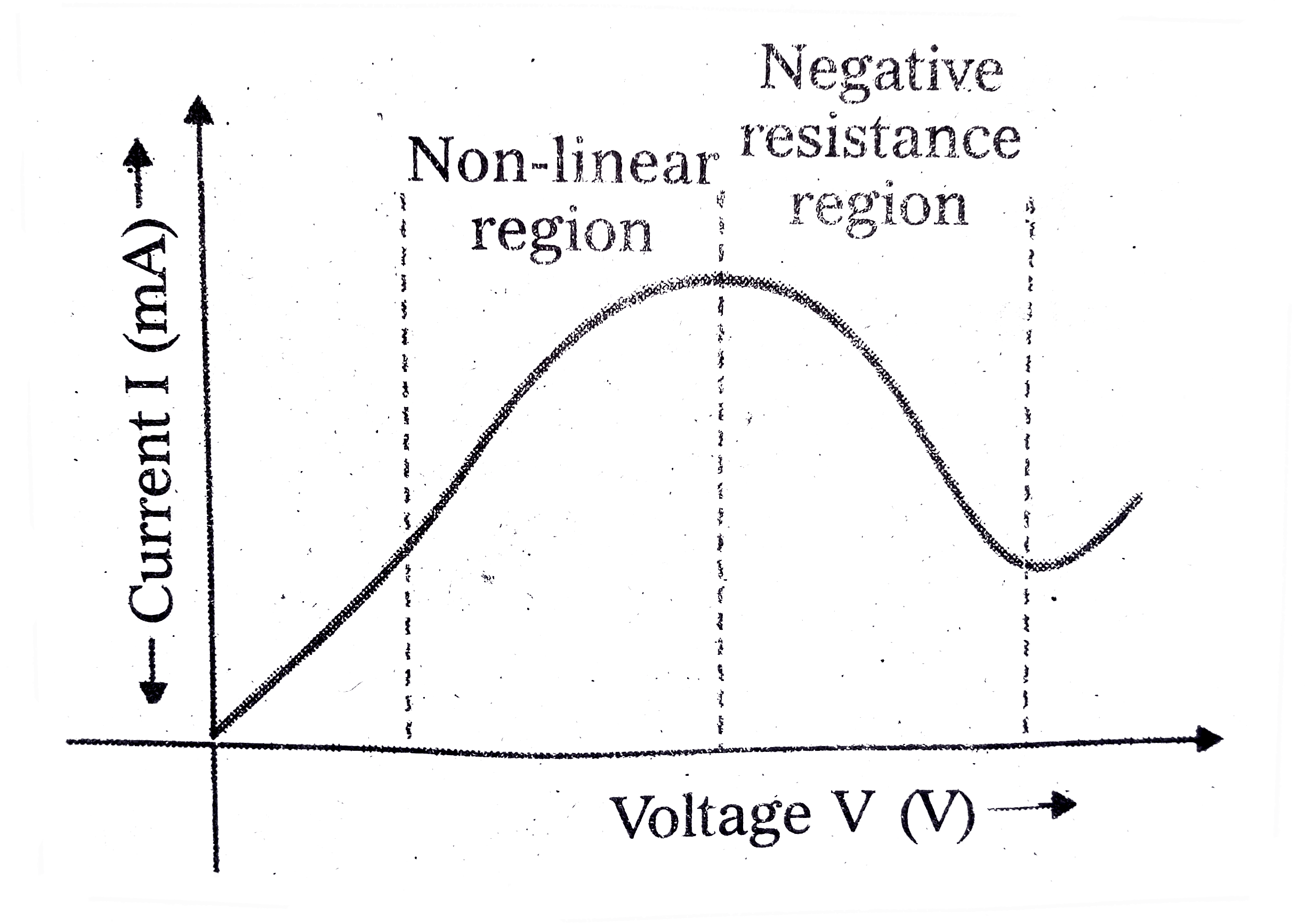
Show the variation of current versus voltage graph for GaAs and mark the I Non-liner region (ii) Negative resistance region.
The relation between V and 1 is not unique. That is, there is more than one value of V for the same current I. material exhibiting such behaivour is GaAs (i.e., alight emitting diode)
Similar Questions
Graph showing the variation of current versus voltage for a material GaAs is shown in figure. Identify the region of (i) negative resistance (ii) where Ohm's law is obeyed.
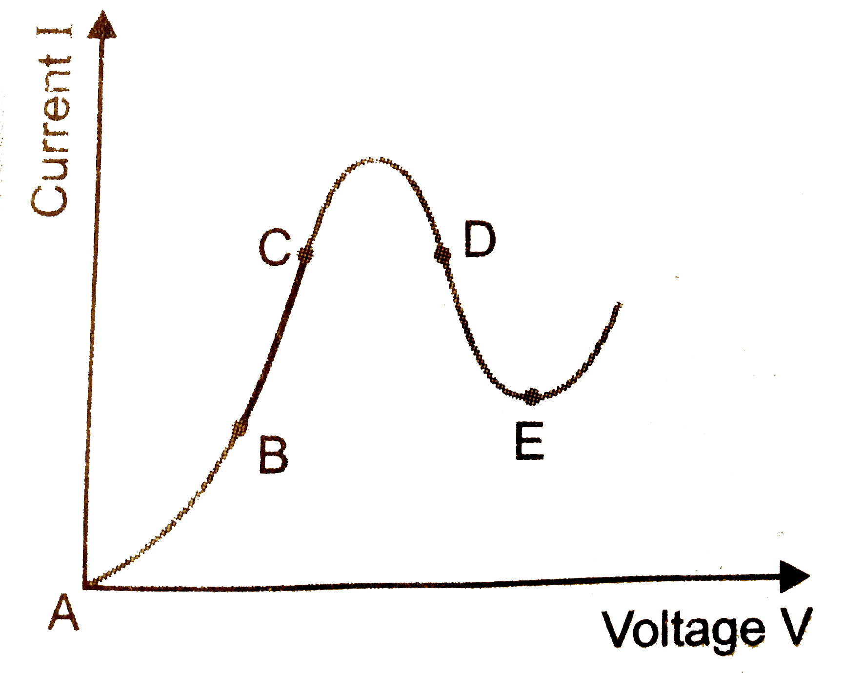
View SolutionGraph showing the variation of current versus voltage for a material GaAs is shown in figure. Identify the region of (i) negative resistance (ii) where Ohm's law is obeyed.

View SolutionIs the graph showing variation of current versus voltage for a diode linear or non-linear?
View SolutionGraph showing the variation of current versus voltage for a material Ga As (a semiconductor) is shown in the Fig. Identify the region of (i) negative resistance, (ii) where Ohm's law is obeyed.
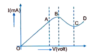
View SolutionPlot a graph showing variation of current versus voltage for the material Ga.
View SolutionPlot a graph showing variation of current versus voltage for the material Ga.
View SolutionPlot a graph showing variation of current versus voltage for the material GaAs
View Solution(a) Draw graph showing the variation of current versus voltage in an electroyte when an external resistance is also connceted.
(b) (i) The graph between resistance (R ) and temperature (T) for Hg is shown in the figure (a). Explain the behaviour of Hg near 4k.
(ii) In which region of the graph shown in the figure (b) is the resistance negative and why?

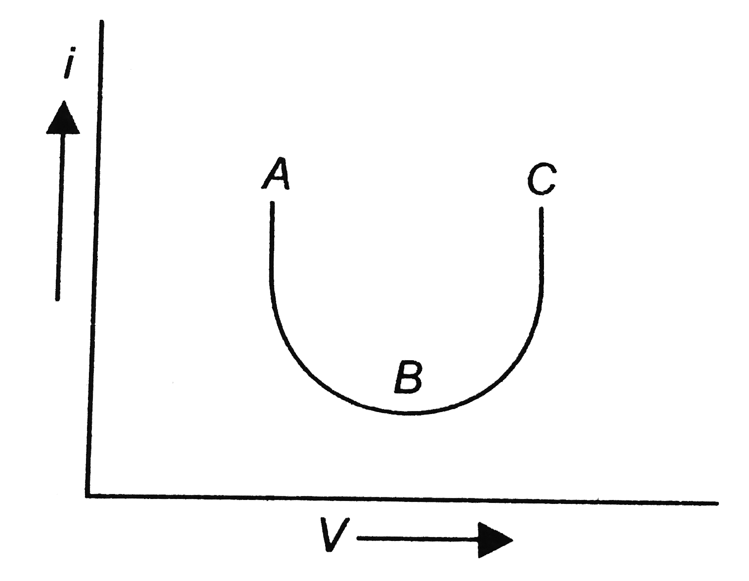
View SolutionThe current-voltage graph of a device is shown in figure. The resistance is negative in region.
View Solution

