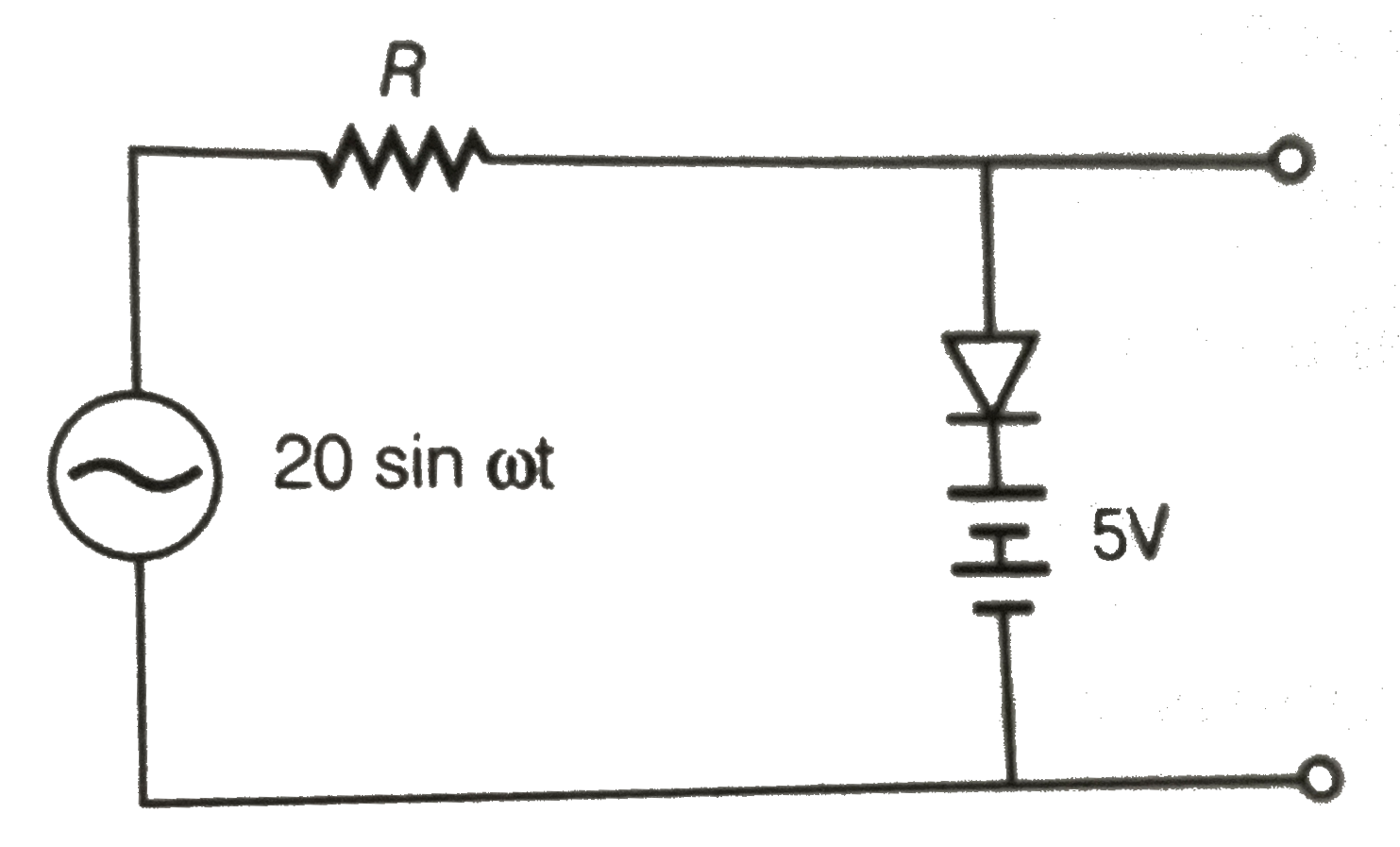
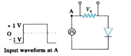
Draw the output waveform across the resistor (Fig.)
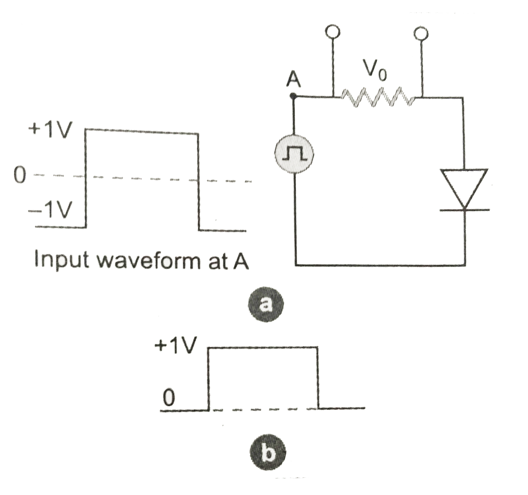
A p-n junction offers low resistance when forward biased and high resistance, when reverse biased. Therefore, there will be output voltage for the positive half cycle of a.c. voltage used as input. Which is shown in Fig.
Similar Questions
Knowledge Check
A square wave (-1 to +1V) is applied to a P-N junction diode as shown. Draw the output wave form across the diode which is assumed to be ideal-
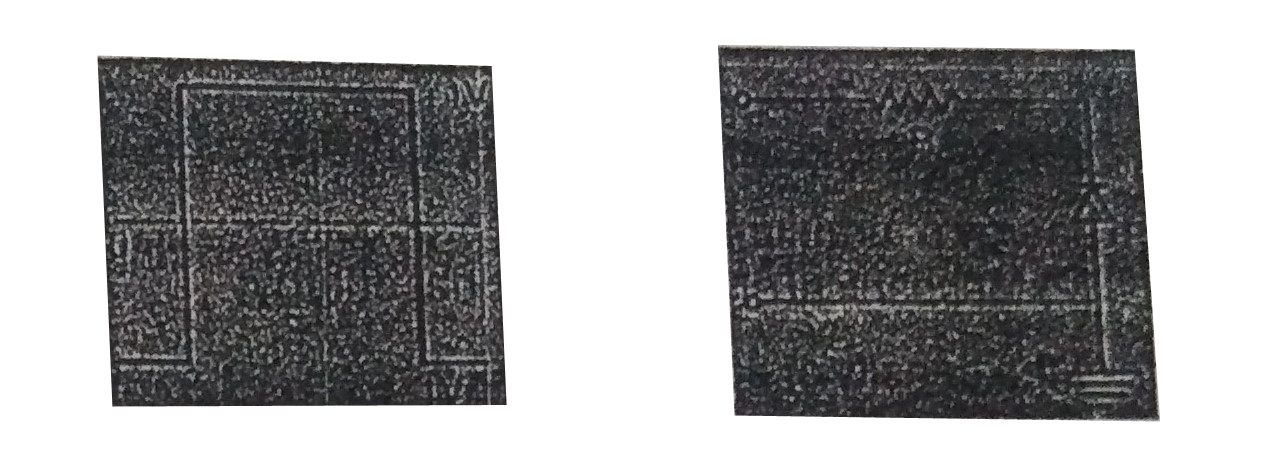 A
A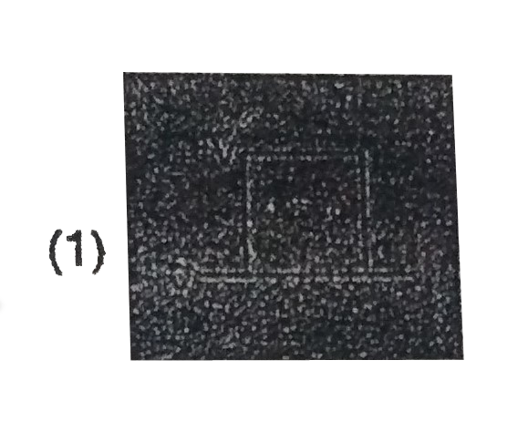 B
B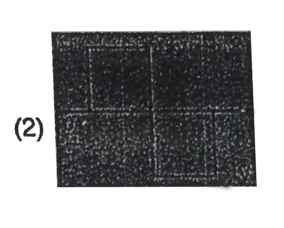 C
C D
D
Draw and explain the output waveform across the load resistor R, if the input wave from is as shown in Fig.

View SolutionDraw and explain the output waveform across the load resistor R, if the input waveform is as shown in the given.
View SolutionWrite the output waveform for the gates
View SolutionAssuming the ideal diode, draw the output waveform for the circuit given in Fig.Explain the waveform.
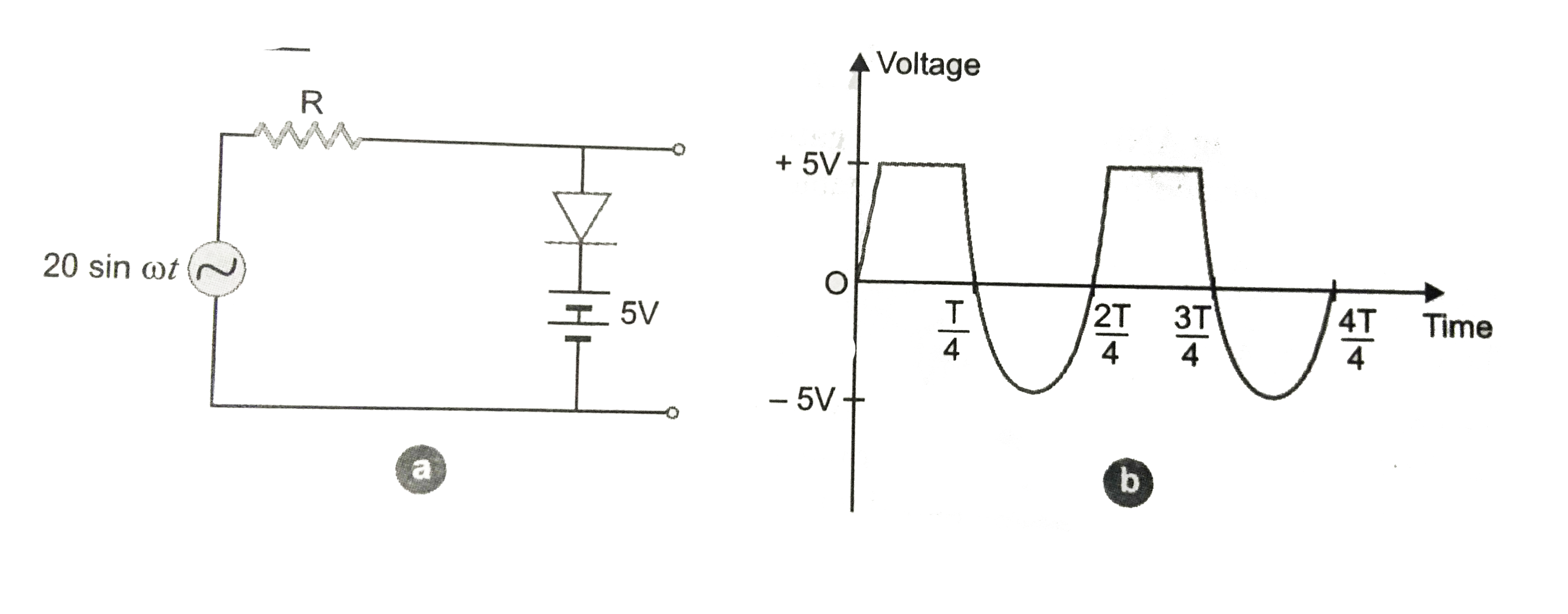
View SolutionAssuming the ideal diode, draw the output waveform for the circuit given in fig. (a), explain the waveform
View Solution

(a) Draw the circuit diagram of reversed bias p-n junction.
(b). Draw the output wavefrom across diode in given circuit.
(c). Draw the truth table for the given logic gate.
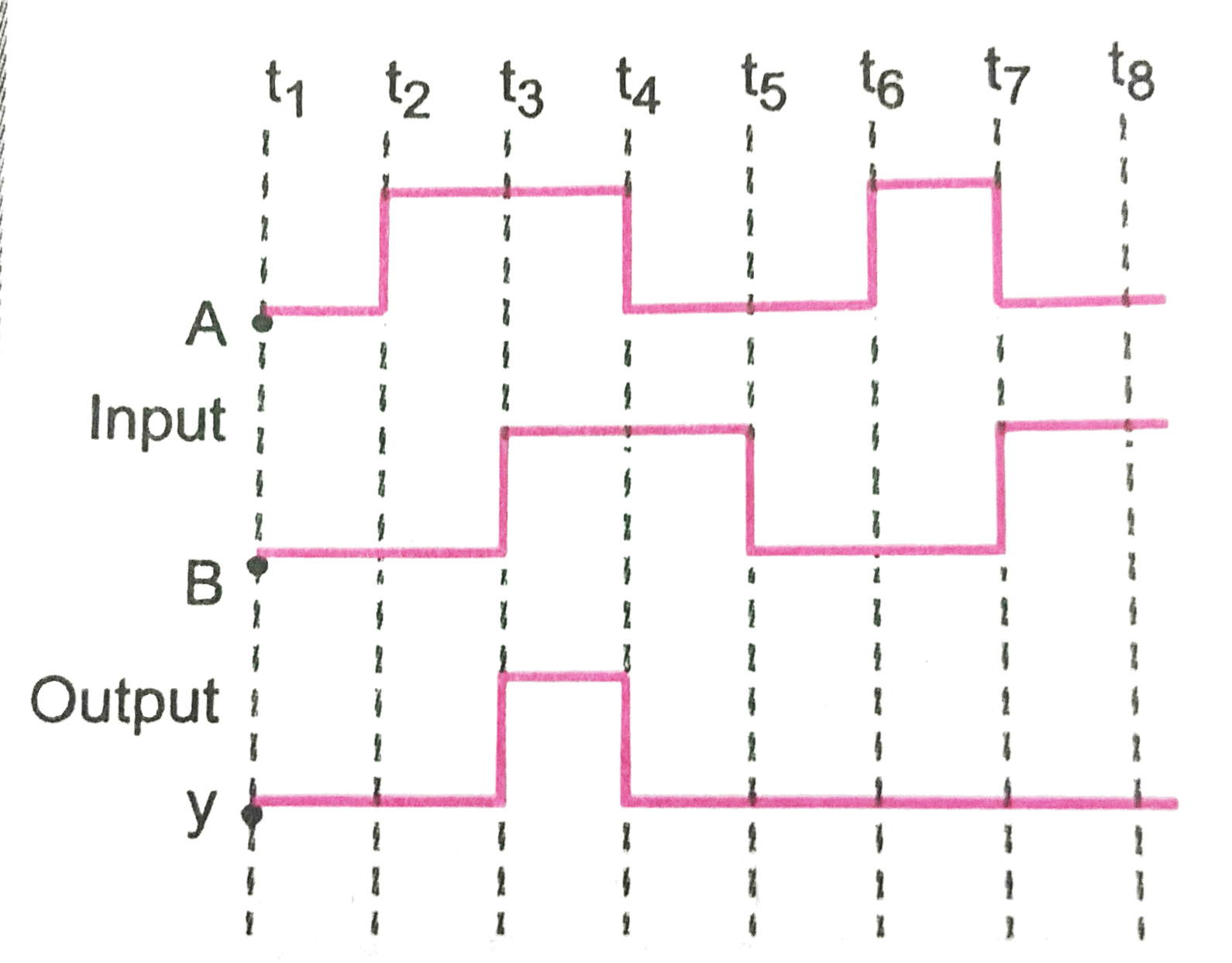
View SolutionThe Fig.shows the input wavwforms A and B for 'AND' gate. Draw the output waveform and write the truth table for this logic gate.
View Solution


_S01_097_Q01.png)