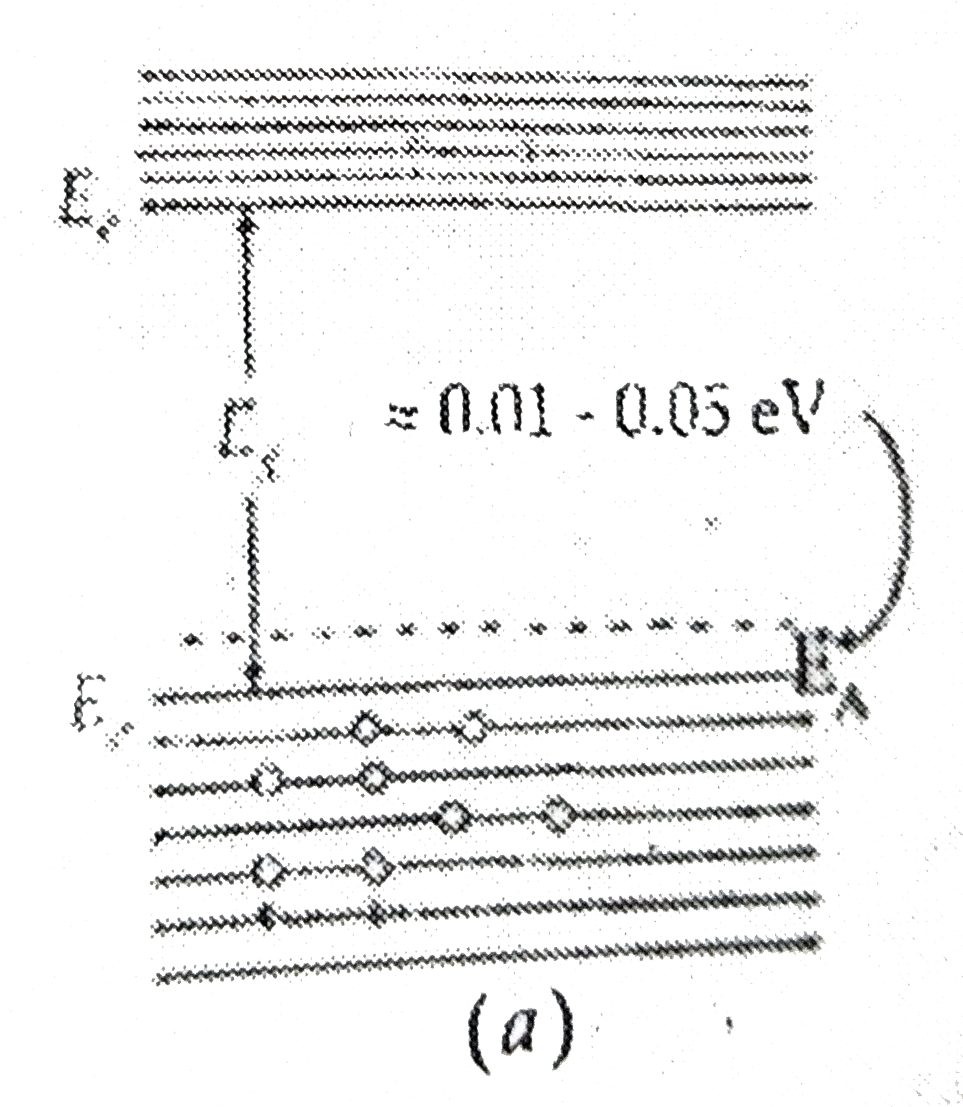
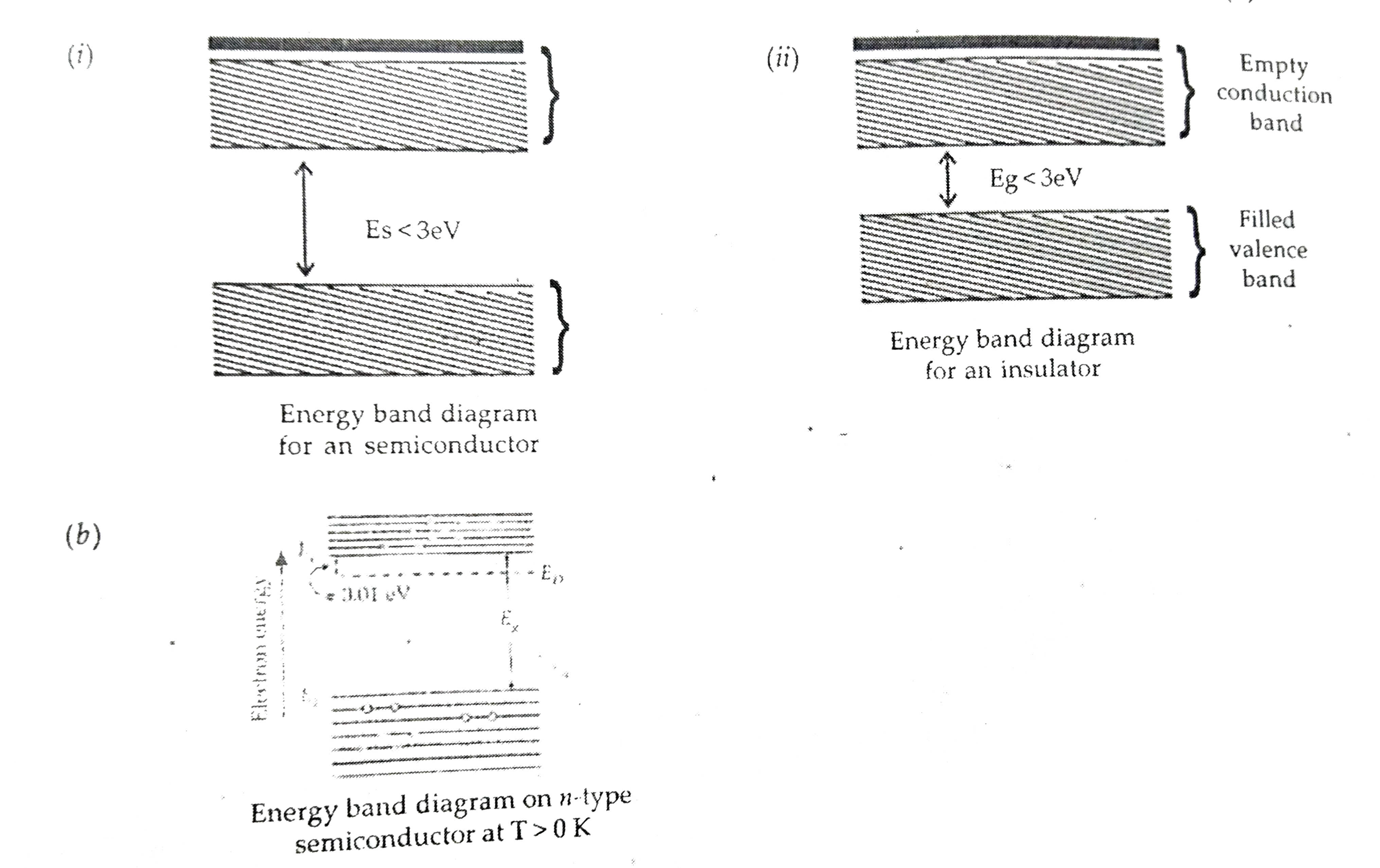
Draw the Energy bands 'diagrams for a (i) pure semiconductor , (ii) insulator , How does the energy band, for a pure semiconductor , get affected when this semiconductor is doped with (a) an acceptor impurity
(b) donor impurity ? Hence discuss why the 'holes' and the 'electrons' respectively, become the 'majority change carries' in these two cases ?
Write the two processes involved in the formation of p−n junction.

Text Solution
In a p-type semiconductor every doped atom has 3 electrons so it makes bonds with 3e of silicon but there is lack of one i.e., one hole is created. So, holes becomes majority carries.
Same way in n type every donor atom add one extra electron and it gives rise to n type semiconductor which has majority carriers as electrons.


|
Similar Questions
ठोसो मे ऊर्जा बैण्ड के निर्माण की व्याख्या कीजिए I (i) एक चालक (ii) एक नैज अर्द्धचालक के लिए ऊर्जा बैण्ड आरेख बनाइए।
View SolutionA pure semiconductor when doped with a donor impurity is called ?
View SolutionDraw energy band diagram of conductors, semiconductors and insulators.
View SolutionCompare conductor, semiconductor, and Insulator by discussing their energy bands .
View SolutionA semiconductor is doped with an acceptor impurity
View SolutionWhat is energy band gap of a semiconductor? How does the energy gap in an intrinsic semiconductor vary, when droped with a trivalent impurity?
View SolutionA semiconductor is doped with an acceptor impurity
View SolutionHow does the energy gap in a semiconductor vary, when doped with a pentavalent impurity?
View Solution

