Explain the reverse characteristics of p-n junction diode by circuit diagram with graph. Solution in Gujrati
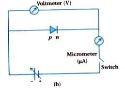
The circuit arrangement for reverse characteristics of the p-n junction diode is shown in the figure (b).

The battery is connected to the diode through a potentiometer or reheostat so that the applied voltage to the diode can be changed.
For different values of voltages, the value of the current is noted. A graph between V and I is obtained as in figure (c ) question 30. Here current is of the order of μA.
The current under reverse bias is essentially voltage independent upto a critical reverse bias voltage known as breakdown voltage Vbr.
When reverse bias voltage becomes equal to break down voltage (V=Vbr), the diode reverse current increases sharply. Even or slight increase in the bias voltage causes large change in the current.
If the reverse current is not limited by an external circuit below the rated value, the p-n junction will get destroyed. Once it exceeds the rated value, the diode gets destroyed due to overheating.
For the diode in reverse bias, the current is very small (−μA) with opposite direction and almost remains constant with change in bias. It is called reverse saturation current.
The general purpose diode are not used beyond the reverse saturation current region.
For diode, a quantity called dynamic resistance as the ratio of small change in voltage ΔV to a small change in current ΔI
rd=ΔVΔI
The resistance of the diode in forward bias mode is approximately between 10Ω to 100Ω in reverse bias mode it is about of the order 106Ω(MΩ).
Similar Questions
Explain the forward characteristics of the p-n junction diode by drawing circuit and graph.
View SolutionExplain briefly with the help of necessary diagram, the forward and the reverse biasing of p-n junction diode. Also draw their characteristic curves in the two cases.
View SolutionWith the help of circuit diagram, explain theV-l characteristics of p-n junction diode in forward biasing.
View SolutionWith the help of circuit diagram, explain theV-l characteristics of p-n junction diode in reverse biasing.
View SolutionDraw the experimental circuit arrangement for studying V-I characteristics of a p-n junction diode in forward and reverse bias.
View SolutionDraw circuit diagrams of forward biased and reverse biased p-n junctions. Describe the use of p-n junction diode as a half-wave rectifier.
View SolutionWith neat circuit diagram, discuss the forward and reverse biasing of a p-n junction diode. Draw their characteristic curves.
View Solution
