The forbidden energy band gap in conductors, semiconductors and insulators are EG1,EG2 and EG3 respectively. The relation among them is
EG1=EG2=EG3
EG1<EG2<EG3
EG1>EG2>EG3
EG1<EG2>EG3
The correct Answer is:B
To solve the question regarding the forbidden energy band gaps in conductors, semiconductors, and insulators, we can follow these steps:
Step 1: Understand the Concept of Energy Band Gaps
The energy band gap (EG) is the energy difference between the valence band and the conduction band in a material. It determines how easily electrons can move from the valence band to the conduction band, which in turn affects the electrical conductivity of the material.
Step 2: Analyze the Band Structure of Conductors, Semiconductors, and Insulators
- Conductors: In conductors, the conduction band and the valence band overlap. This means that there is no energy gap (EG1 ≈ 0). Electrons can easily flow, allowing conductors to conduct electricity efficiently.
- Semiconductors: In semiconductors, there is a small energy gap (EG2). This gap allows some electrons to jump from the valence band to the conduction band at room temperature, enabling semiconductors to conduct electricity, but not as freely as conductors.
- Insulators: In insulators, the energy gap (EG3) is large. This means that at room temperature, it is very difficult for electrons to jump from the valence band to the conduction band, resulting in very poor conductivity.
Step 3: Establish the Relationship Among the Energy Band Gaps
From the analysis:
- EG1 (Conductor) is the smallest, as there is effectively no gap.
- EG2 (Semiconductor) is larger than EG1 but smaller than EG3.
- EG3 (Insulator) is the largest, as it represents a significant barrier for electron movement.
Thus, the relationship among the energy band gaps is:
EG1<EG2<EG3
Final Answer
The relation among the forbidden energy band gaps in conductors, semiconductors, and insulators is:
EG1<EG2<EG3
---
The energy band gap (EG) is the energy difference between the valence band and the conduction band in a material. It determines how easily electrons can move from the valence band to the conduction band, which in turn affects the electrical conductivity of the material.
- Conductors: In conductors, the conduction band and the valence band overlap. This means that there is no energy gap (EG1 ≈ 0). Electrons can easily flow, allowing conductors to conduct electricity efficiently.
- Semiconductors: In semiconductors, there is a small energy gap (EG2). This gap allows some electrons to jump from the valence band to the conduction band at room temperature, enabling semiconductors to conduct electricity, but not as freely as conductors.
From the analysis:
- EG1 (Conductor) is the smallest, as there is effectively no gap.
- EG2 (Semiconductor) is larger than EG1 but smaller than EG3.
- EG3 (Insulator) is the largest, as it represents a significant barrier for electron movement.
EG1<EG2<EG3
The relation among the forbidden energy band gaps in conductors, semiconductors, and insulators is:
EG1<EG2<EG3
Topper's Solved these Questions
- SEMICONDUCTORSBook:RESONANCE ENGLISHChapter:SEMICONDUCTORSExercise:Exercise 2
Explore 16 Videos
- SEMICONDUCTORSBook:RESONANCE ENGLISHChapter:SEMICONDUCTORSExercise:Exercise 3
Explore 88 Videos
- SEMICONDUCTORSBook:RESONANCE ENGLISHChapter:SEMICONDUCTORSExercise:Exercise 3
Explore 88 Videos
- REVISION DPPBook:RESONANCE ENGLISHChapter:REVISION DPPExercise:All Questions
Explore 463 Videos
- SIMPLE HARMONIC MOTION Book:RESONANCE ENGLISHChapter:SIMPLE HARMONIC MOTION Exercise:Advanced Level Problems
Explore 13 Videos
Similar Questions
The depletion layer in diode is 1μm wide and the knee potential is 0.6V, then the electric field in the depletion layer will be
View SolutionWhen p−n junction diode is forward biased, then
View SolutionWhen p−n junction diode is forward biased, then
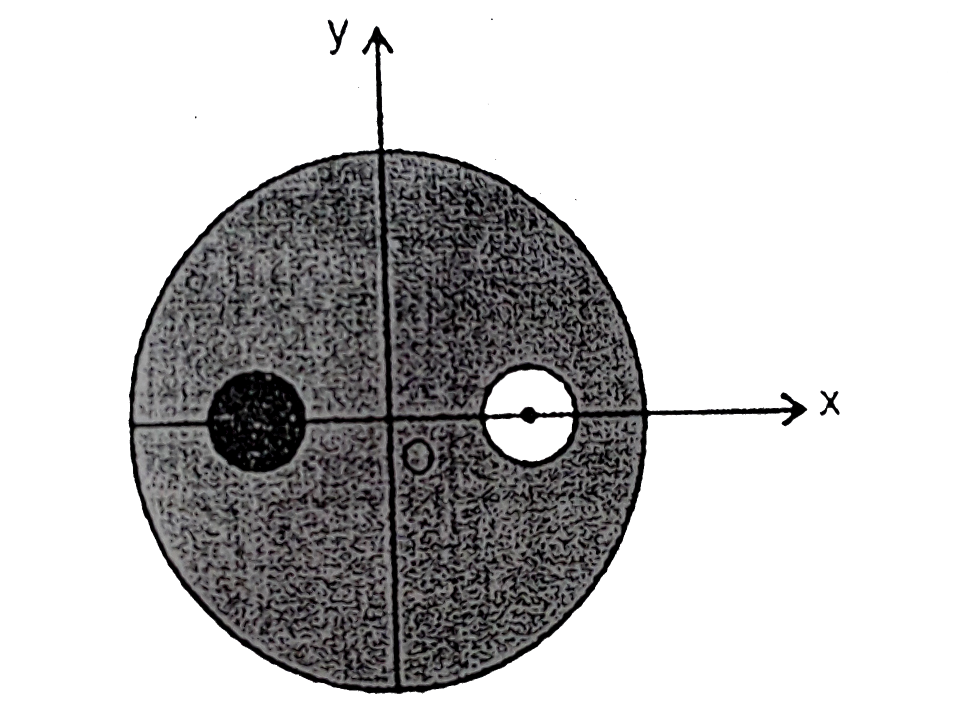
View SolutionConsider a solid sphere of density ρ and radius 4R. Centre of the sphere is at origin. Two spherical cavities centred at (2R,0) and (−2R,0) are created in sphere. Radii of both cavities is R. In left cavity material of density 2ρ is filled while second cavity is kept empty. What is gravitational field at origin.

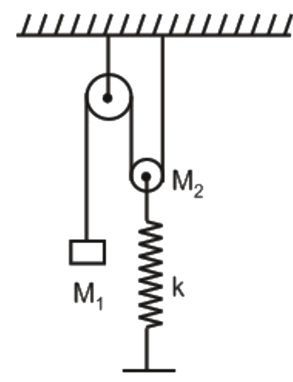
View SolutionA block of mass M1 is constrained to move along with a moveable pulley of mass M2 which is connected to a sprin of force constant k, as shown in the figure. If the mass of the fixed pulley is negligible and friction is absent everywhere, then the period of small oscillations of the system is

View SolutionThe forbidden energy band gap in conductors, semiconductors and insulators are EG_(1), EG_(2) and EG_(3) respectively. The relation among them is
View SolutionThe forbidden energy band gap in conductors, semiconductors and insulators are EG_(1), EG_(2) and EG_(3) respectively. How are they related?
View SolutionWhich is the correct relation for forbidden energy gap in conductor, semi conductor and insulator
View SolutionThe forbidden energy band gap in semi conductor , conductor and insulator are E_(1),E(2)and E_(3) , respectively. The relation among them is
View Solutionयदि वर्जित ऊर्जा बैंड अंतराल (forbidden energy band) का मान चालक, अर्ध-चालक एवं अचालक के लिए क्रमश: EG1,EG2 व EG3 हो तो ये किस प्रकार सम्बंधित होंगे?
View SolutionThe forbidden energy gap in conductors , semiconductors and insulators are EG_1 , EG_2 and EG_3 respectively . The relation among them is :
View SolutionThe band gaps of a conductor, semiconductor and insulator are respectively Eg_(1), and Eg_(2) and Eg_(3) . The relationship between them can be given as ………
View SolutionBandgap of conductive, semiconductor and insulating materials, respectively Eg_(1) , Eg_(2) And Eg_(3) Is. And the relationship between these three bandgaps ................
View SolutionThe forbidden energy gap is conductors, semiconductors and insulators are Delta_(1), Delta_(2) and Delta_(3) , respectively. The relations among them is
View SolutionThe forbidden energy band gap in conductors semiconductors and insulators are EG_1, EG_2 and EG_3 respectively. The relation among them is
View Solution
