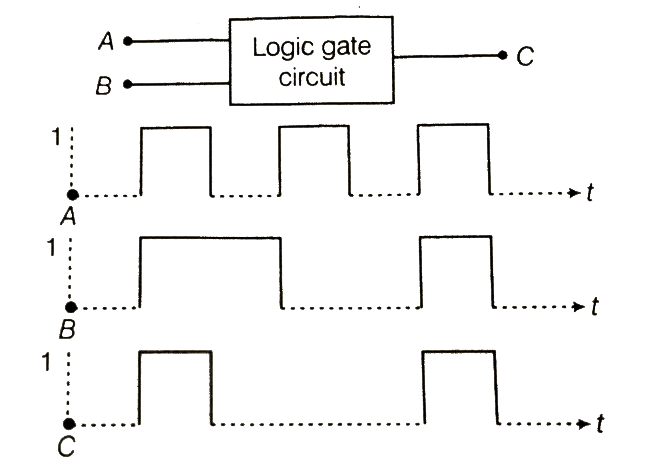
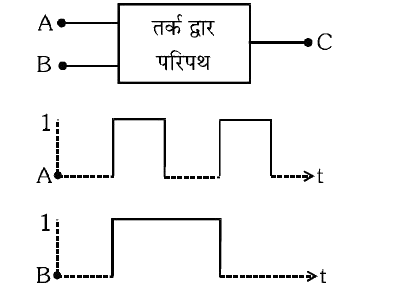
The figure shows a logic circuit with two inputs A and B and the output C. The voltage wave forms across A, B and C are as given. The logic circuit gate is
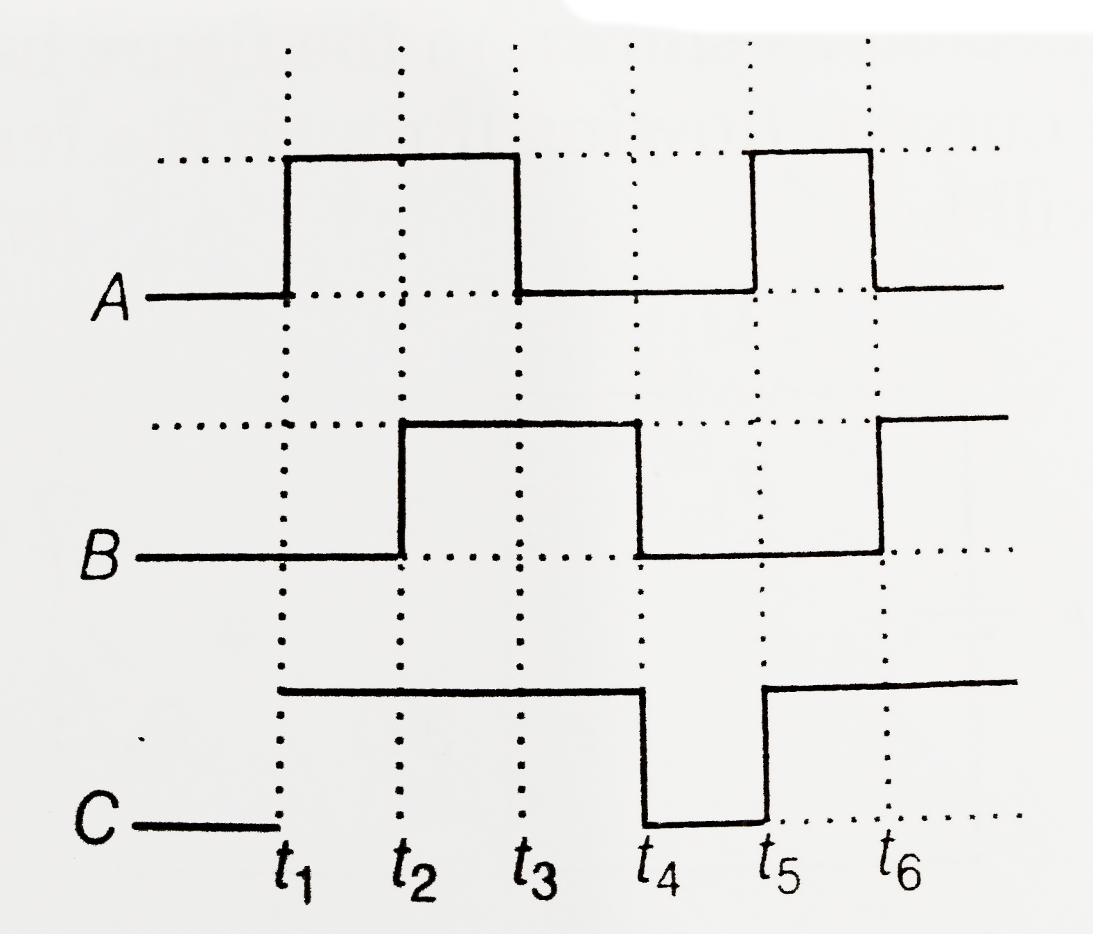
OR gate
NOR gate
AND gate
NAND gate
The correct Answer is:A
Step by step video solution for The figure shows a logic circuit with two inputs A and B and the output C. The voltage wave forms across A, B and C are as given. The logic circuit gate is by Physics experts to help you in doubts & scoring excellent marks in Class 12 exams.
Updated on:21/07/2023Topper's Solved these Questions
- SEMICONDUCTORSBOOK - RESONANCE ENGLISHCHAPTER - SEMICONDUCTORSEXERCISE - Exercise 2
16 Videos
- REVISION DPPBOOK - RESONANCE ENGLISHCHAPTER - REVISION DPPEXERCISE - All Questions
463 Videos
- SIMPLE HARMONIC MOTION BOOK - RESONANCE ENGLISHCHAPTER - SIMPLE HARMONIC MOTION EXERCISE - Advanced Level Problems
13 Videos
Similar Questions
The depletion layer in diode is 1μm wide and the knee potential is 0.6V, then the electric field in the depletion layer will be
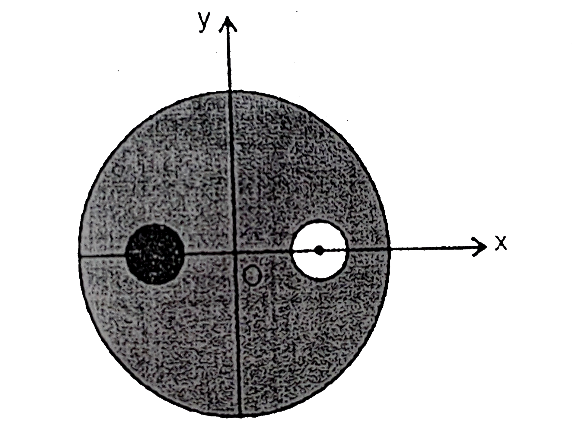
View SolutionConsider a solid sphere of density ρ and radius 4R. Centre of the sphere is at origin. Two spherical cavities centred at (2R,0) and (−2R,0) are created in sphere. Radii of both cavities is R. In left cavity material of density 2ρ is filled while second cavity is kept empty. What is gravitational field at origin.
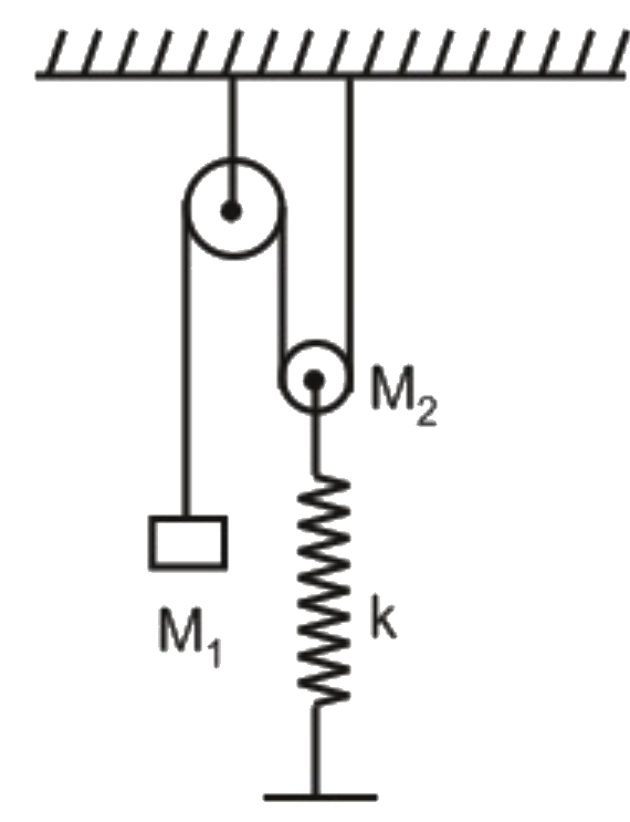
View SolutionA block of mass M1 is constrained to move along with a moveable pulley of mass M2 which is connected to a sprin of force constant k, as shown in the figure. If the mass of the fixed pulley is negligible and friction is absent everywhere, then the period of small oscillations of the system is
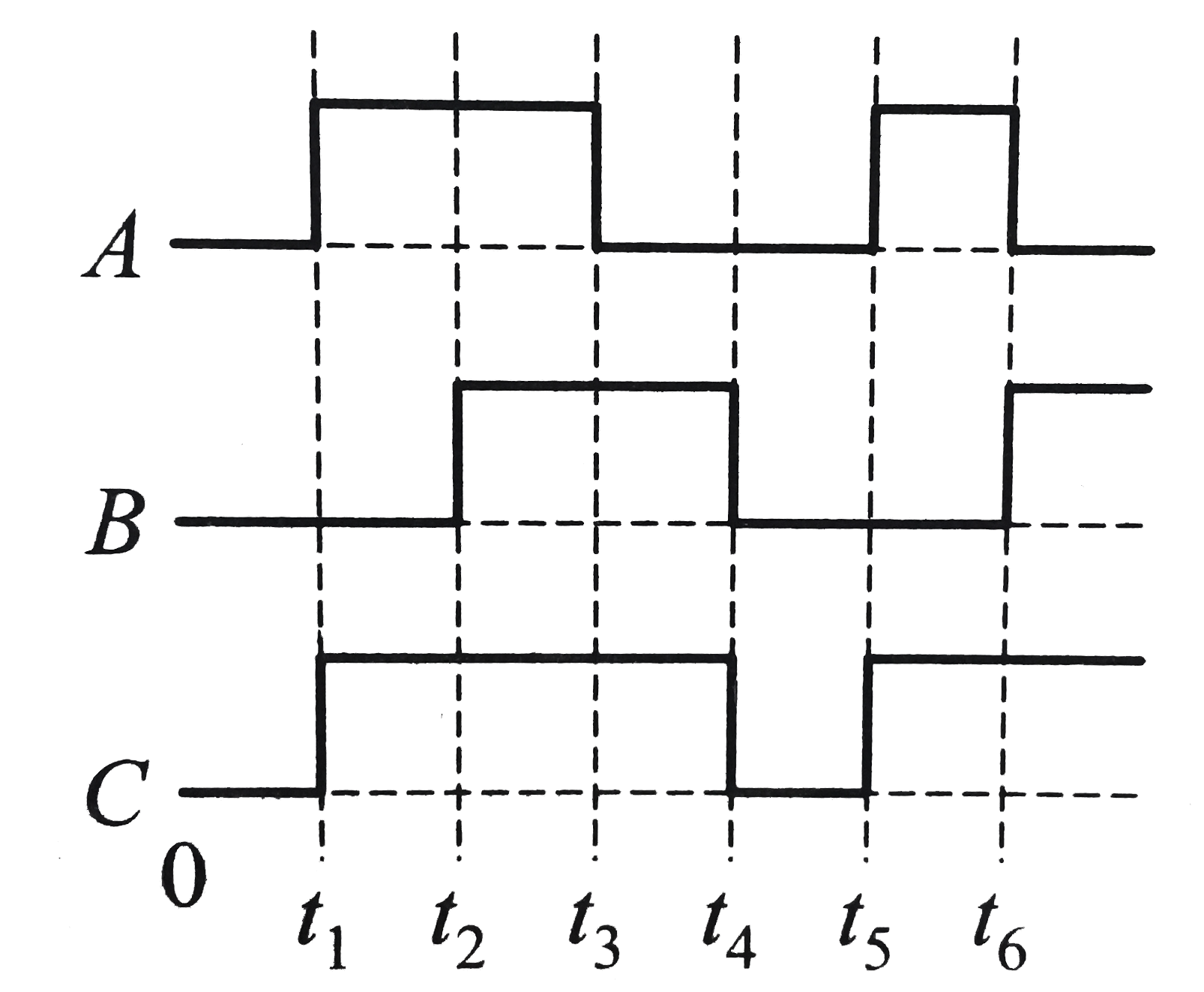
View SolutionThe figure shows a logic circuit with two inputs A and B and the output C. The voltage wave forms across A,B and C are as given. The logic circuit gate is
View SolutionFig, shows a logic gate circuit with two input A and B and the output C. The voltage wave form of A, B and C are as shown in Fig.The logic gate circuit is
View SolutionThe following figure shows a logic gate circuit with two inputs A and B output C. The voltage waveforms of A,B and C are as shown in second figure given below :-
_E01_436_Q01.png)
The logic circuit gate is :-
View SolutionThe following figure shows a logic gate circuit with two inputs A and B and the output C. The voltage waveforms of A, B and C are as shown below.
The logic circuit gate is
View Solutionचित्र में एक लॉजिक परिपथ में दो निवेशी A तथा B और एक निर्गत C दर्शाया गया है| A,B तथा C के वोलटता तरंगरूप दिए गए अनुसार है| तब लॉजिक परिपथ गेट है-
View Solutionनिम्नलिखित चित्र में एक तर्क द्वार परिपथ को दिखाया गया है जिसमें दो निवेश A और B और एक निर्गत हैं। A,B और C के वोल्टता तरंग-रूप निम्न प्रकार हैं
यह तर्क परिपथ द्वार है
View SolutionThe following shows a logic gate circuit with two inputs A and B and the output C. The voltage waveforms of A, B and C are as shown below.
The logic circuit gate is
View Solutionनिम्नलिखित चित्र में एक AND तर्क द्वार परिपथ को दिखाया गया है जिसमें दो निवेश A और B और एक निर्गत C हैं। C की वोल्टता का तरंग-रूप निम्न प्रकार होगा
View SolutionThe figure shows the voltage waveforms across two inputs A and B and the output Y of a logic circuit. The logic circuit gate is
View SolutionThe figure shows a logic circuit with two inputs A and B and the output C. The voltage wave forms across A,B and C are as given. The logic circuit gate is

View SolutionThe following figure shows a logic gate circuit with two inputs A and B and the output Y. The voltage waveforms of A,B and Y are as given :
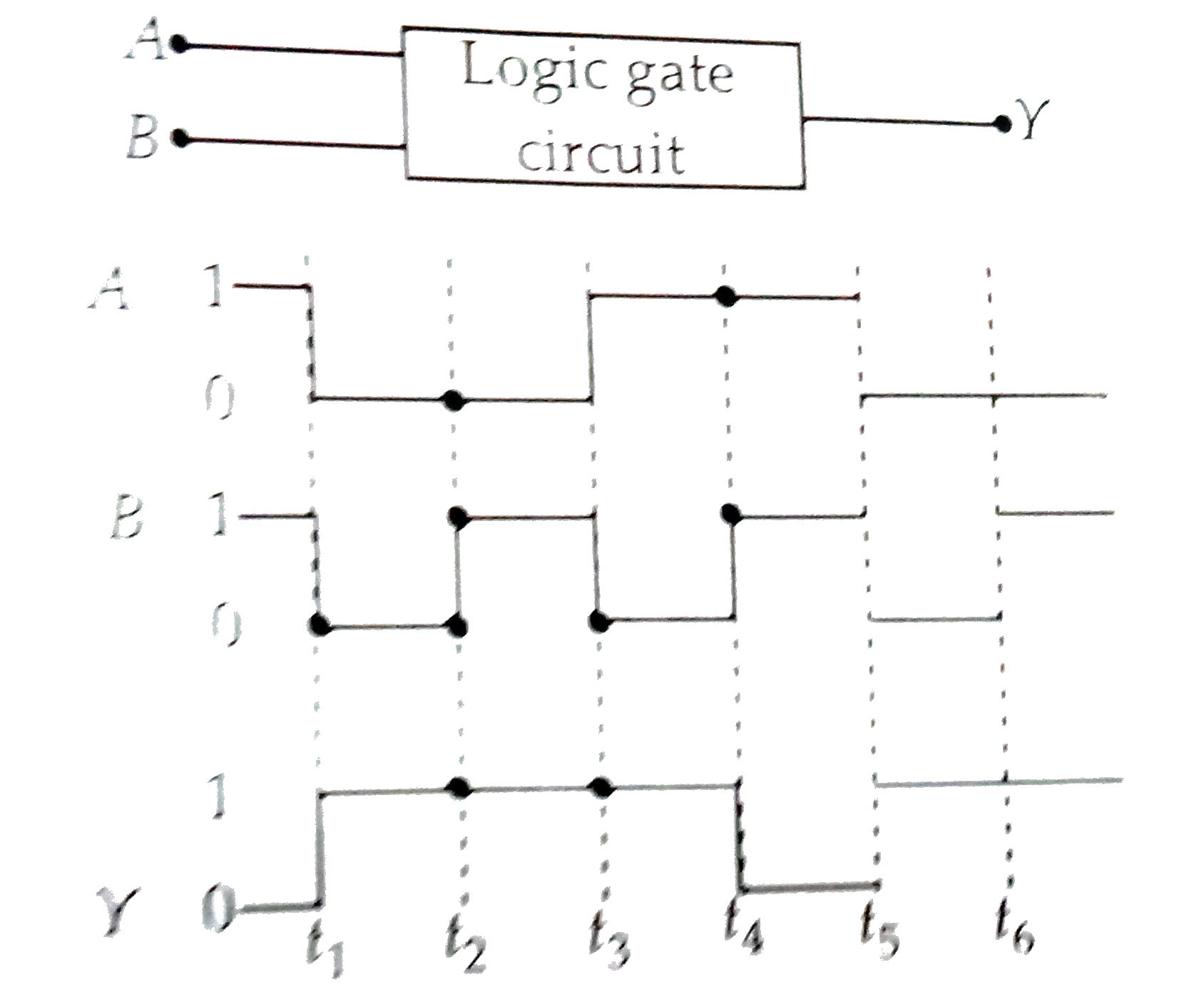
The logic gate is
View SolutionThe figure shows a logic circuit with two inputs A and B and the output C. The voltage wave forms across A,B and C are as given. The logic circuit gate is

View SolutionThe following figure shows a logic gate circuit with two inputs A and B output C. The voltage waveforms of A,B and C are as shown in second figure given below :-
_E01_436_Q01.png)
The logic circuit gate is :-
View Solution

