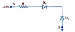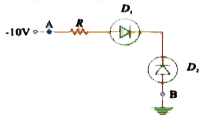
In figure, assuming the diodes to be ideal, Solution in Gujrati
D1 is forward biased and D2 is reverse biased and hence current flows from A to B
D2 is forward biased and D1 is reverse biased and hence no current flows from B to A and vice versa.
D1 and D2 are both forward biased and hence current flows from A to B.
D1andD2 are both reverse biased and hence no current flows from A to B and vice versa.
The correct Answer is:B
D2 is forward biased and D1 is reverse biased and hence no current flows from B to A and vice versa.
For diode D1,VA=−10VandVK=0⇒VA<VR⇒D1 is reverse biased. Hence its resistance would be R1=∞(∵D1 is an ideal diode)
For diode D2,VA=0andVK=−10V⇒VA>VK⇒D2 is forward biased. Hence its resistance would be R2=0.(∵D2 is an ideal diode)
Here, D1andD2 are connected in series and so its equivalent resistance R=R1+R2=∞+0=∞ and so current will not flow, neither from A to B nor from B to A.
⇒ Option (B) is correct.
Topper's Solved these Questions
- SEMICONDUCTOR ELECTRONICS : MATERIALS, DEVICES AND SIMPLE CIRCUITS Book:KUMAR PRAKASHANChapter:SEMICONDUCTOR ELECTRONICS : MATERIALS, DEVICES AND SIMPLE CIRCUITS Exercise:Section-C: NCERT Exemplar Solution (Multiple Choice Qustion (More than One Options))
Explore 8 Videos
- SEMICONDUCTOR ELECTRONICS : MATERIALS, DEVICES AND SIMPLE CIRCUITS Book:KUMAR PRAKASHANChapter:SEMICONDUCTOR ELECTRONICS : MATERIALS, DEVICES AND SIMPLE CIRCUITS Exercise:Section-C: NCERT Exemplar Solution (Very Short Answer Type Questions)
Explore 6 Videos
- SEMICONDUCTOR ELECTRONICS : MATERIALS, DEVICES AND SIMPLE CIRCUITS Book:KUMAR PRAKASHANChapter:SEMICONDUCTOR ELECTRONICS : MATERIALS, DEVICES AND SIMPLE CIRCUITS Exercise:Section-B : Numericals (Numerical From .DARPAN. Based On Textbook)
Explore 14 Videos
- SAMPLE QUESTION PAPER Book:KUMAR PRAKASHANChapter:SAMPLE QUESTION PAPER Exercise:PART-B SECTION-C
Explore 5 Videos
- WAVE OPTICSBook:KUMAR PRAKASHANChapter:WAVE OPTICSExercise:SECTION-D (MULTIPLCE CHOICE QUESTIONS (MCQS)) (MCQS FROM DARPAN BASED ON TEXTBOOK)
Explore 239 Videos
Similar Questions
When an electric field is applied across a semiconductor
View SolutionWhy are elemental dopants for Silicon on Germanium usually chosen from group XIII on group XV ?
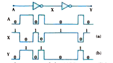
View SolutionA logic circuit is shown in the diagram. Draw the output signal at the point X and Y for the input signal shown in the figure at point A.

View SolutionTwo charges –q and +q are located at points (0, 0, –a) and (0, 0, a), respectively.
(a) What is the electrostatic potential at the points (0, 0, z) and (x, y, 0) ?
(b) Obtain the dependence of potential on the distance r of a point from the origin when r/a>>1 .
(c) How much work is done in moving a small test charge from the point (5,0,0) to (–7,0,0) along the x-axis? Does the answer change if the path of the test charge between the same points is not along the x-axis?
View SolutionAccording to particle theory of light what is the velocity of light in a dense medium, compared to that in rare medium ?
View SolutionIn figure , assuming the diodes to be ideal ,
View SolutionAssuming that the junction diode is ideal the current through the diode is :-
View SolutionAssuming that the junction diode is ideal, the current in arrangement shown in figure is
View SolutionIn a figure given alongside assuming the diodes to be ideal

View SolutionAssuming that the function diode is ideal, the current in the arrangement shown in figure is .
View SolutionAssuming that the junction diode is ideal, the current in arrangement shown in figure is

View SolutionFour silicon diodes are connected as shown in the figure. Assuming the diodes to be ideal. The current through the resistor R is
View SolutionIn Fig 1.50 assuming the diodes to be ideal

View SolutionIn Fig assuming the diodes to be ideal :

View SolutionAssuming that the junction diode is ideal , in the circuit shown here , the current through the diode is :
View Solution
