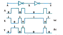
A logic circuit is shown in the diagram. Draw the output signal at the point X and Y for the input signal shown in the figure at point A.
 Solution in Gujrati
A

B

C

D

Video Solution
Text Solution
The correct Answer is:D
At the forward bias connection of p-n junction from RL value of input signal is 5V in output. For input signal -5V negative voltage of input we are not getting output.
∴ (D) is correct option.
|
Similar Questions
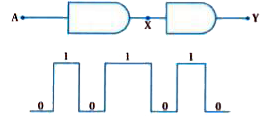
A circuit of logic gte made from two AND gate is shown in following figure. Draw output waves for point X. For A and for Y.

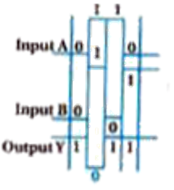
View SolutionThe figure shows the input signal A, input signal B and output signal Y. Which logic gate does it represent ?

View Solutionनीचे दिए हुए चित्र में एक तार्किक द्वार का संकेत तथा दो निवेशी संकेत A व B दर्शाये गये है।

निर्गत तरंग संकेत बनाइये।
View Solution
input are given as shown

then output signal is-
View SolutionThe output Y of the logic circuit as shown in figure is
View SolutionThe output (X) of the logic circuit shown in figure will be
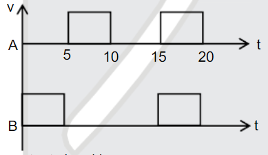
View SolutionThe real-time changes of input signals A and B are as shown in the figure. If the input is sent to the NAND gate, select the output signal from the following.
View SolutionThe output (X) of the logic circuit shown in figure will be
View Solution
